(Hong Kong)

Product Summary
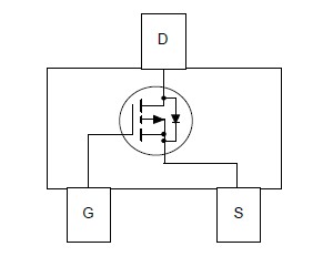
The NDS356AP is a p-channel logic level enhancement mode field effect transistor. This very high density process is especially tailored to minimize on-state resistance. The NDS356AP is particularly suited for low voltage applications such as notebook computer power management, portable electronics, and other battery powered circuits where fast high-side switching, and low in-line power loss are needed in a very small outline surface mount package.
Parametrics
NDS356AP absolute maximum ratings: (1)VDSS Drain-Source Voltage: -30 V; (2)VGSS Gate-Source Voltage - Continuous: ±20 V; (3)ID Maximum Drain Current - Continuous: ±1.1 A; - Pulsed: ±10A; (4)PD Maximum Power Dissipation: 0.5 W; (5)TJ,TSTG Operating and Storage Temperature Range: -55 to 150 ℃.
Features
NDS356AP features: (1)-1.1 A, -30 V, RDS(ON) = 0.3 Ω @ VGS=-4.5 V; RDS(ON) = 0.2 Ω @ VGS=-10 V; (2)Industry standard outline SOT-23 surface mount package using proprietary SuperSOTTM-3 design for superior thermal and electrical capabilities; (3)High density cell design for extremely low RDS(ON); (4)Exceptional on-resistance and maximum DC current capability.
Diagrams
| Image | Part No | Mfg | Description |  |
Pricing (USD) |
Quantity | ||||
|---|---|---|---|---|---|---|---|---|---|---|
 |
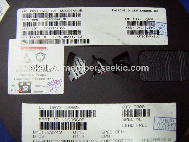
 NDS356AP |
Fairchild Semiconductor |
MOSFET P-Channel Logic |
Data Sheet |
Negotiable |
|
||||
 |
NDS356AP_L99Z |
Fairchild Semiconductor |
MOSFET P-Ch LL FET Enhancement Mode |
Data Sheet |
Negotiable |
|
||||